- 您现在的位置:买卖IC网 > Sheet目录868 > LTM4613MPV#PBF (Linear Technology)IC UMODULE DC/DC 8A 133-LGA
�� �
�
�LTM4613�
�APPLICATIONS� INFORMATION�
�V� OUT(MARGIN)� =�
�?� V� OUT�
�R� PGM� =�
�V� OUT� 1.18V�
�V� OUT�
�(� R� fSET� ||� 133k� )�
�1.5� ?� 10� ?� 10�
�Table1.R� FB� Standard1%ResistorValuesvsV� OUT�
�V� OUT� (V)� 3.3� 5� 6� 8� 10� 12� 14� 15�
�R� FB� (kΩ)� 22.1� 13.7� 11� 8.06� 6.34� 5.23� 4.42� 4.12�
�The� MPGM� pin� programs� a� current� that� when� multiplied�
�by� an� internal� 10k� resistor� sets� up� the� 0.6V� reference� ±�
�offset� for� margining.� A� 1.18V� reference� divided� by� the�
�R� PGM� resistor� on� the� MPGM� pin� programs� the� current.�
�Calculate� V� OUT(MARGIN)� :�
�%V� OUT�
�100�
�Where� %V� OUT� is� the� percentage� of� V� OUT� to� be� margined,�
�and� V� OUT(MARGIN)� is� the� margin� quantity� in� volts:�
�?� ?� 10k�
�0.6V� V� OUT(MARGIN)�
�Where� R� PGM� is� the� resistor� value� to� place� on� the� MPGM�
�pin� to� ground.�
�The� output� margining� will� be� ±� margining� of� the� value.�
�This� is� controlled� by� the� MARG0� and� MARG1� pins.� See�
�the� truth� table� below:�
�Operating� Frequency�
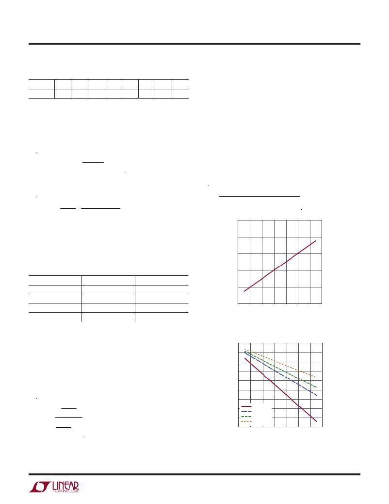
�The� operating� frequency� of� the� LTM4613� is� optimized� to�
�achieve� the� compact� package� size� and� the� minimum�
�output� ripple� voltage� while� still� keeping� high� efficiency.�
�As� shown� in� Figure� 2,� the� frequency� is� linearly� increased�
�with� larger� output� voltages� to� keep� the� low� output� cur-�
�rent� ripple.� Figure� 3� shows� the� inductor� current� ripple� ?I�
�with� different� output� voltages.� In� most� applications,� no�
�additional� frequency� adjusting� is� required.�
�If� lower� output� ripple� is� required,� the� operating� frequency�
�f� can� be� increased� by� adding� a� resistor� R� fSET� between� f� SET�
�pin� and� SGND,� as� shown� in� Figure� 19.�
�f� =�
�1000�
�800�
�600�
�400�
�MARG1�
�MARG0�
�MODE�
�LOW�
�LOW�
�NO� MARGIN�
�200�
�LOW�
�HIGH�
�HIGH�
�LOW�
�MARGIN� UP�
�MARGIN� DOWN�
�0�
�2�
�4�
�6�
�8�
�10�
�12�
�14�
�16�
�HIGH�
�HIGH�
�NO� MARGIN�
�OUTPUT� VOLTAGE� (V)�
�4613� F02�
�Parallel� Operation�
�The� LTM4613� device� is� an� inherently� current� mode� con-�
�trolled� device.� This� allows� the� paralleled� modules� to� have�
�very� good� current� sharing� and� balanced� thermal� on� the�
�design.� Figure� 21� shows� a� schematic� of� the� parallel� design.�
�The� voltage� feedback� equation� changes� with� the� variable�
�N� as� modules� are� paralleled.� The� equation:�
�Figure� 2.� Operating� Frequency� vs� Output� Voltage�
�9�
�8�
�7�
�6�
�5�
�4�
�V� OUT�
�?� 1�
�R� F� B� =�
�100k�
�N�
�0.6V�
�3�
�2�
�1�
�0�
�2�
�4�
�V� IN� =� 16V�
�V� IN� =� 24V�
�V� IN� =� 28V�
�V� IN� =� 36V�
�6� 8� 10� 12�
�OUTPUT� VOLTAGE� (V)�
�14�
�16�
�where� N� is� the� number� of� paralleled� modules.�
�4613� F03�
�Figure� 3.� Pk-Pk� Inductor� Current� Ripple� vs� Output� Voltage�
�4613f�
�11�
�发布紧急采购,3分钟左右您将得到回复。
相关PDF资料
LTM4614IV#PBF
IC UMODULE DC/DC DUAL 4A 144LGA
LTM4615IV#PBF
IC SWIT REG BUCK 4A ADJ 144LGA
LTM4618IV#PBF
IC DC-DC UMODULE BUCK 6A 84-LGA
LTM4619IV#PBF
IC SWIT REG BUCK 4A ADJ 144LGA
LTM4627MPY#PBF
IC DC/DC UMODULE 15A 133-BGA
LTM4628EV#PBF
IC DC/DC UMODULE 16A 144-LGA
LTM8008HV#PBF
IC DC/DC UMODULE 16-LGA
LTM8020IV#PBF
IC DC/DC UMODULE 200MA 21-LGA
相关代理商/技术参数
LTM4614
制造商:LINER 制造商全称:Linear Technology 功能描述:Dual 4A per Channel Low VIN DC/DC μModule Regulator
LTM4614EV
制造商:LINER 制造商全称:Linear Technology 功能描述:Dual 4A per Channel Low VIN DC/DC μModule Regulator
LTM4614EV#PBF
功能描述:IC UMODULE DC/DC DUAL 4A 144LGA RoHS:是 类别:电源 - 板载 >> DC DC Converters 系列:µModule® 设计资源:VI-200, VI-J00 Design Guide, Appl Manual 标准包装:1 系列:* 类型:隔离 输出数:1 电压 - 输入(最小):66V 电压 - 输入(最大):160V Voltage - Output 1:12V Voltage - Output 2:- Voltage - Output 3:- 电流 - 输出(最大):* 电源(瓦) - 制造商系列:50W 电压 - 隔离:* 特点:* 安装类型:通孔 封装/外壳:9-FinMod 尺寸/尺寸:4.60" L x 1.86" W x 0.79" H(116.8mm x 47.2mm x 20.1mm) 包装:散装 工作温度:-25°C ~ 85°C 效率:* 电源(瓦特)- 最大:*
LTM4614EV#PBF
制造商:Linear Technology 功能描述:DC/DC Module IC
LTM4614EVPBF
制造商:Linear Technology 功能描述:Dual 4A Channel DC/DC UModule Regulator
LTM4614IV
制造商:LINER 制造商全称:Linear Technology 功能描述:Dual 4A per Channel Low VIN DC/DC μModule Regulator
LTM4614IV#PBF
功能描述:IC UMODULE DC/DC DUAL 4A 144LGA RoHS:是 类别:电源 - 板载 >> DC DC Converters 系列:µModule® 设计资源:VI-200, VI-J00 Design Guide, Appl Manual 标准包装:1 系列:* 类型:隔离 输出数:1 电压 - 输入(最小):66V 电压 - 输入(最大):160V Voltage - Output 1:12V Voltage - Output 2:- Voltage - Output 3:- 电流 - 输出(最大):* 电源(瓦) - 制造商系列:50W 电压 - 隔离:* 特点:* 安装类型:通孔 封装/外壳:9-FinMod 尺寸/尺寸:4.60" L x 1.86" W x 0.79" H(116.8mm x 47.2mm x 20.1mm) 包装:散装 工作温度:-25°C ~ 85°C 效率:* 电源(瓦特)- 最大:*
LTM4614IVPBF
制造商:Linear Technology 功能描述:Conv DC-DC Dual Step-Down 5.5V LGA144